The Christmas tree in the pictures above is 14 centimetres long. Since it is made of graphene, it consists of carbon atoms in only one layer and is only a third of a nanometer thick. It is cut out of a 10-meter long roll of graphene, transferred in one piece using a rebuilt laminating machine and then scanned with terahertz radiation.
The experiment shows that continuous quality control can be done during the production of graphene, which is expected to play a significant role in future high-speed electronics, i.e. medical instruments and sensors.
Graphene is a so-called two-dimensional material, i.e. it consists of atoms in one cohesive layer that is only one atom thin. It is more robust, stiffer and better at conducting electricity and heat than any other material we know of. Therefore, graphene is an obvious candidate for electronic circuits that take up less space, weigh less, are bendable and are more efficient than the electronics we know today.
“Even if you could make a pencil drawing of a Christmas tree and lift it off the paper—which, figuratively, is what we have done—it would be much thicker than one atom. A bacterium is, e.g. 3000 times thicker than the graphene layer we used. That’s why I dare call this the world’s thinnest Christmas tree. And although the starting point is carbon, just like the graphite in a pencil, graphene is at the same time even more conductive than copper. The “drawing” is made in one perfect layer in one piece, “ says Professor Peter Bøggild who lead the team behind the Christmas tree experiment.
“But behind the Christmas joke hides an important breakthrough. For the first time, we managed to make an in-line quality control of the graphene layer while we transferred it. Doing this is the key to gaining stable, reproducible and usable material properties, which is the prerequisite for utilising graphene in, e.g. electronic circuits.“
30,000 times thinner than kitchen film
As the researchers have done in this case, the graphene can be “grown” on copper film. The graphene is deposited on a roll of copper foil at around 1000 ° C. That process is well known and well-functioning. But a lot can go wrong when the ultra-thin graphene film is moved from the copper roller to where it is used. Since graphene is 30,000 times thinner than kitchen film, it is a demanding process. Researcher Abhay Shivayogimath has been behind several new inventions in DTU’s transfer process, ensuring a stable transfer of the graphene layers from the copper roll.
Moreover, there has been no technology that could control the electrical quality of graphene on the go - while transferring it. This yearPeter Bøggild and his colleague Professor Peter Uhd Jepsen from DTU Fotonik, one of the world’s leading terahertz researchers, established a way to do it.
The coloured images are measurements of how the graphene layer absorbs terahertz radiation. The absorption is directly related to the electric conductivity: the better the conductive graphene, the better it absorbs.
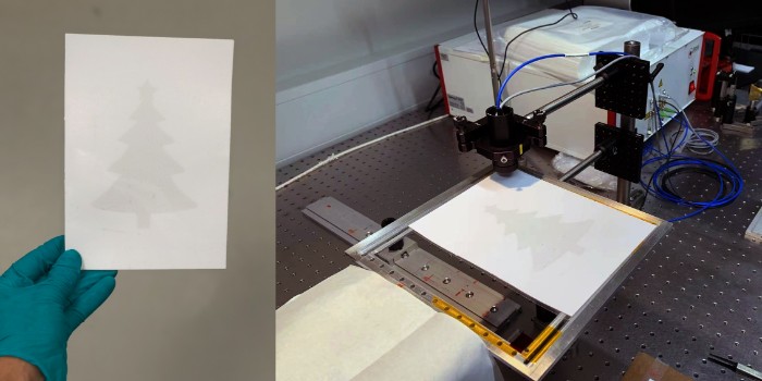
Here, the graphene layer is seen after transfer from the copper roll and while being examined using terahertz radiation. Illustration: Abhay Shivayogimath og Jie Ji.
Terahertz rays are high-frequency radio waves that lie between infrared radiation and microwaves. Like X-rays, they can be used to scan human bodies, as we know it from airport security. Terahertz rays can also take pictures of the electrical resistance of the graphene layer. By connecting the terahertz scanner to the machine that transfers the graphene film, it is possible to image the electrical properties of the film during the transfer process.
Official international measurement standard
Suppose the implementation of graphene and other 2D materials is to be accelerated. In that case, ongoing quality assurance is a prerequisite, says Peter Bøggild. Quality control precedes trust, he says. The technology can guarantee that graphene-based technologies are manufactured more uniformly and predictably with fewer errors. This year, the DTU researchers’ method was approved as the first official international measurement standard for graphene. Their method was described earlier this year in the article Terahertz imaging of graphene paves the way to industrialisation.
The potential is excellent. Graphene and other two-dimensional materials can e.g. enable the manufacturing of high-speed electronics performing lightning-fast calculations with far less power consumption than the technologies we use today. But before graphene can become more widespread on an industrial scale and be used in electronics, we encounter in everyday life three main problems must be solved.
First, the price is too high. More and faster production is needed to bring the price down. But with that, you face the second problem: When you increase the speed and can not at the same time check the quality, the risk of error also increases dramatically. At high high-speed transfer, everything must be set precisely.This brings us to the third problem: How do you know what is precise?
It requires measurements. And preferably measurements during the actual transfer process. The DTU team is convinced that the best bet on that method is quality control using terahertz radiation.
Peter Bøggild emphasises that these three problems have not been solved with the new method alone:
“We have taken a very significant step. We have converted a laminating machine into a so-called roll-2-roll transfer system. It gently lifts the graphene layer from the copper roll on which the graphene layer is grown and moves it onto plastic foil without it breaking, becoming wrinkled or dirty. When we combine this with the terahertz system, we can immediately see if the process has gone well. That is, whether we have unbroken graphene with low electrical resistance, ”says Peter Bøggild.
The Terahertz method was created in collaboration with researchers in the Danish innovation fund project TRIM and the large EU research project Graphene Flagship. DTU partakes in Graphene Flagship with the basic research centre Center for Nanostructured Graphene.
In the video below, Peter Bøggild explains the method in detail. On his blog at Ingeniøren, you can read his own description of the experiment (in Danish).