360 degrees
Virtual cleanroom
Visit the virtual 3D model of the cleanroom at DTU Lyngby Campus and take a look around the 1.500 square meters particle-free laboratories.
The microchip has become a key technology in the digital society. Denmark needs robust research environments and large-scale clean rooms for chip production to develop the nano- and microchips of the future.

In an era in which digitalization is becoming increasingly important to the development of our society, and where we depend on stability in a large number of critical functions, there is one tiny thing that has become completely essential to us: the microchip.
There is still a need to develop the technologies used in chip production. There is also a need for continued research, innovation, and education in this area.
The world is becoming increasingly digital, and the chip is the raw material of the digital world. In line with large parts of the world being increasingly based on the existence and continued supply of microchips and nanochips, chip technology becomes a key ingredient. Our energy systems, healthcare sector, communication systems, forms of payment, industry, production, and services are largely based on IT that uses chips.
A shortage of chips for industrial use has arisen in recent years—a veritable chip crisis. DTU cannot remedy this crisis, but—by virtue of the University’s unique facilities—DTU can help meet the chip challenge through research, education of engineers, and development of new prototypes and solutions.
The main manufacturers of mass-produced chips for—for example—mobile phones and computers are located in Asia and the United States. Factories for mass production of chips cost billions of dollars, as this entails very large-scale and demanding manufacturing. In Europe—and not least in Denmark—there is more focus on manufacturing specially developed chips for niche areas such as control of circulation pumps from Grundfos, optical chips for analysis of eye diseases, or special sensors for measuring drinking water quality.
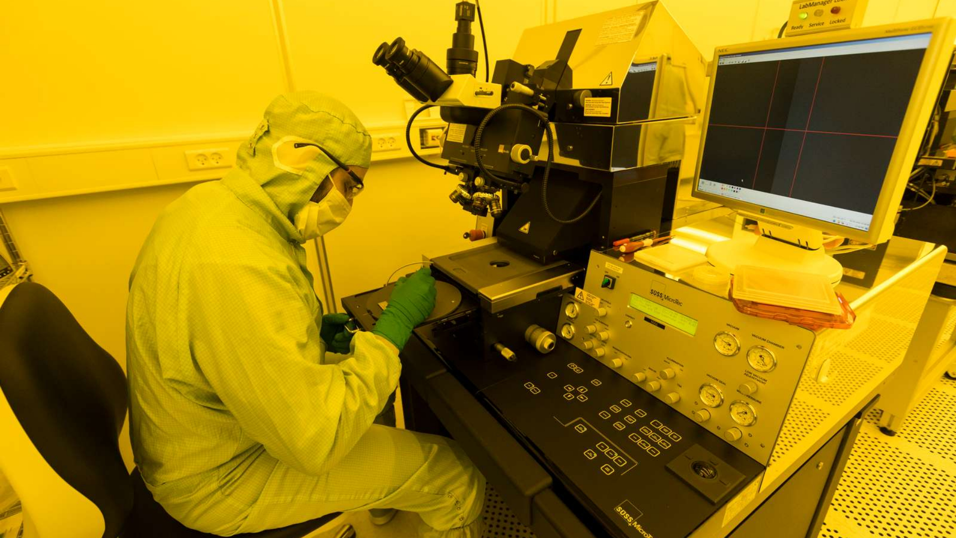
Here, DTU’s clean room has often played a key role as innovation facility.

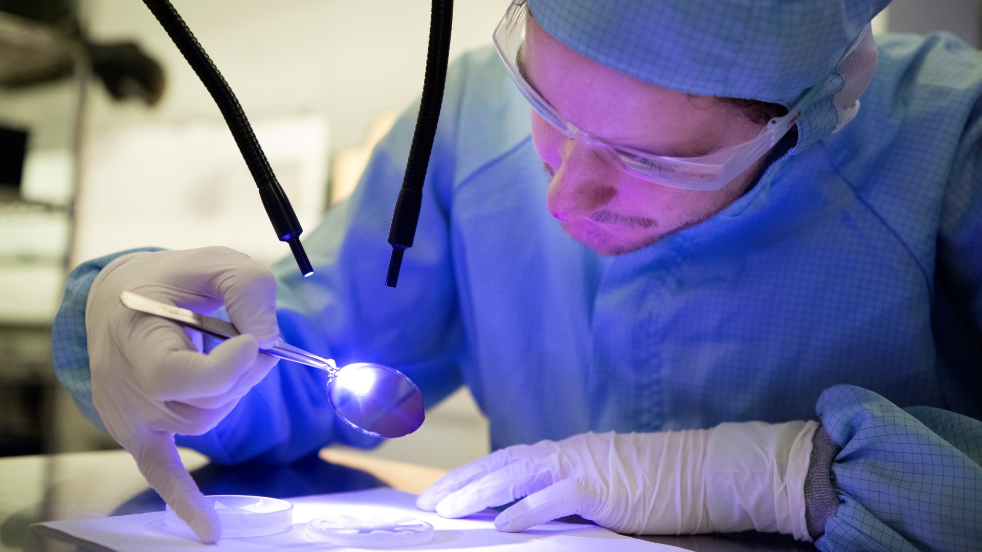
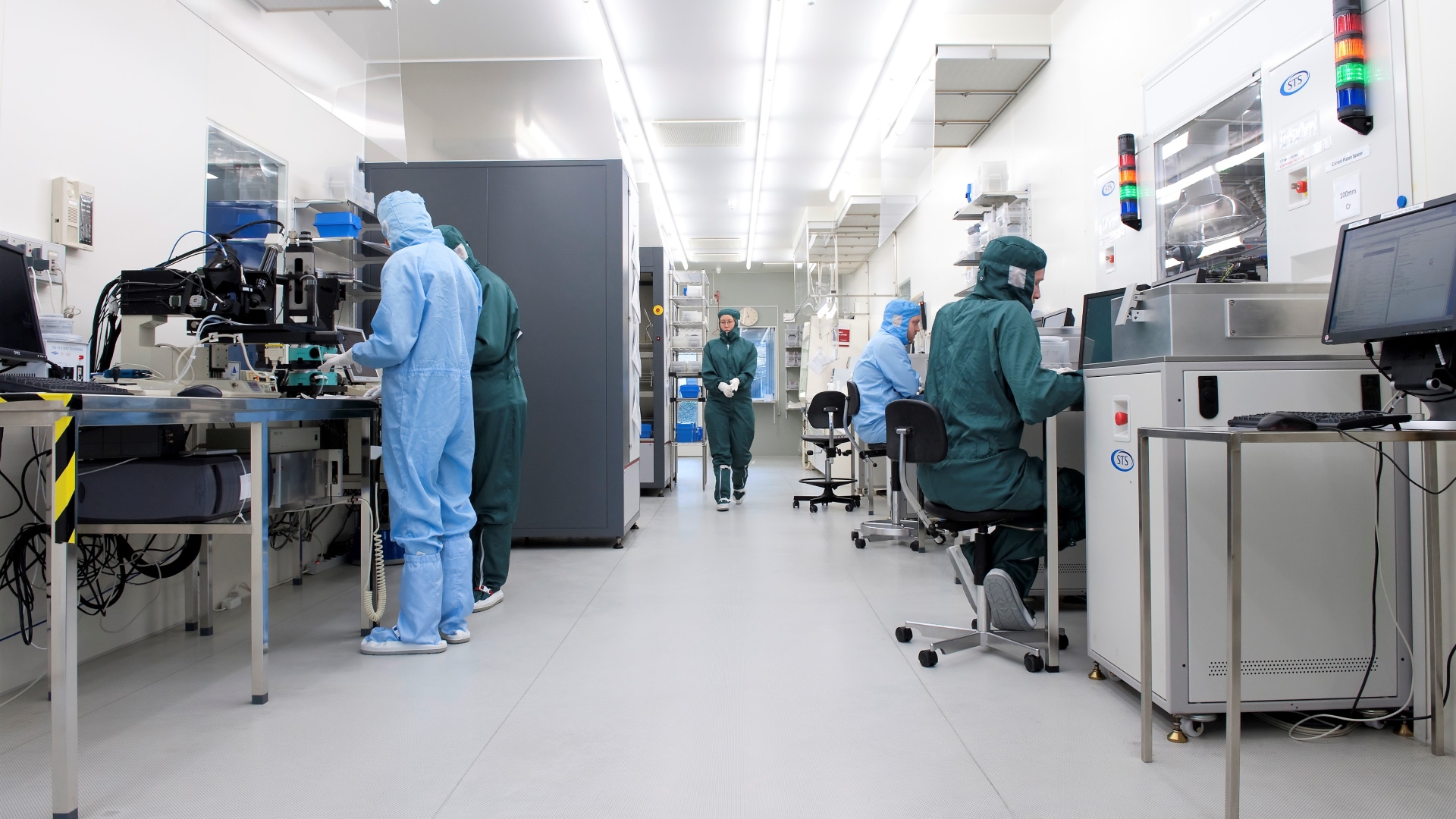
Facilities that meet these extremely high standards are usually only found in the manufacturing industry and in large organizations, but—as something unique—they are also found at DTU in the National Centre for Nano Fabrication and Characterization, which is one of the largest university-owned clean-room facilities in Europe.
DTU Nanolab has at its disposal advanced technical equipment and is one of the few universities with an ISO 9001-certified quality management system for a clean room. DTU Nanolab’s facilities can ensure the transition from research to direct industrial production. DTU is open to companies that want to develop, prototype, and mature their products in our facilities.
Robot-driven wafer handling guarantees a short lead time and thus fast scaling for small batch productions.
Or take our state-of-the-art Deep UV Stepper, which is equipment that is only available at a few universities worldwide. One of them is the EPFL in Switzerland, which is among our partners in the EuroTech Universities Alliance.
A microchip is a collection of electronic circuits on a small flat piece of silicon. These electrical circuits contain transistors. Transistors are small electrical contacts that are controlled by other small electrical contacts—other transistors. When many transistors are connected to each other and can switch on and off quickly enough, a computer chip or microprocessor can be built.
To make such a transistor, small patterns are created on a silicon wafer with addition and removal of materials to create a multilayer structure. Electrical connections to the different parts of the structure are then created using a thin strip of metal.
Silicon is used due to its electrical properties, abundant availability, and low price. It is extracted from ordinary sand consisting of silicon dioxide. By melting the sand, removing the oxygen, and cleaning thoroughly, pure silicon is achieved.
Silicon can act as a semiconductor by changing the electrical properties using small amounts of other elements (typically boron or phosphorus). In some cases, silicon will then behave like an electrical conductor and in other cases like an insulator. These options can be controlled electrically. Electric current can thus be switched on and off with (another) electric current.
Microchips for—for example—mobile phones or computers are following a trend in which they are becoming increasingly small and more and more powerful.
Making the transistors smaller makes it possible to produce a very large quantity of them without using more materials, thus reducing the price per transistor. The more transistors that are located in the same area, the greater the computing power per microchip and the higher the optimization of power consumption.
But the development also means that the machines used in the manufacture of microchips and nanochips become significantly more complicated. Extreme precision is required when using billions of transistors per square centimetre.
The area required for a single transistor has been reduced many thousands of times over the past 35 years. We can now make chips with enormous computing power containing many billions of transistors. The structures have become so fine that we are down to atomic dimensions. Therefore, building a chip factory has become complicated. We need machines that can control structures that are a few hundred atoms in size, and we need to add materials with a thickness of just a few atomic layers. It also makes demands on how small vibirations are tolerated and on the temperature fluctuations to which the machine is exposed.
The transistors on a modern microchip are about 10 nm (one nanometre is one billionth of a metre). It is very difficult to imagine, but—with letters of 50 nm—the entire Bible could be printed approximately 2,000 times on the surface of a grain of rice.
When laying layers on top of each other, the individual layers must be placed very precisely. The slightest vibration makes this impossible. And the temperature must be stable. If the temperature increases by just one degree Celsius, a chip of 1 centimetre will become about 50 nanometres larger, and the next layer will not fit correctly.

360 degrees
Visit the virtual 3D model of the cleanroom at DTU Lyngby Campus and take a look around the 1.500 square meters particle-free laboratories.